PCBCraft tutorial: inspect the LED example and its KiCad export
A six-step documentation guide to connections, footprints, basic routing, checks and separate native and KiCad board files.
Last updated
Menus and supported features can change. Compare the source-check date below with your current app version.
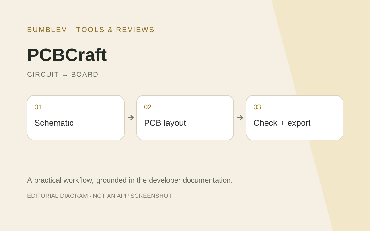
The goal is to inspect the official LED example, then check the native project and KiCad board export. This teaches the documented file flow; it is not a new circuit-design lesson or an execution report.
Prepare
Read the official Rust and system-library requirements for Linux/WSL or native Windows execution. Use a separate test folder and KiCad for checking the exported board. Browser saving is not a supported completion route in the pinned documentation.
| Item | Target |
|---|---|
| Starting point | Official LED example |
| Tabs | Schematic, PCB Layout, Libraries, Checks |
| Editable source | led-test.pcbcraft |
| Exchange file | led-test.kicad_pcb |
| Completion | Reopen files and inspect connectivity and checks |
1. Open the official sample
Use LED example or the documented cargo run -p pcbcraft -- --sample path. Read component references and sample assumptions before changing values. Do not infer a new circuit’s electrical suitability from an editing example.
2. Inspect schematic pins and nets
The README documents A for symbol selection and W for pin-to-pin wiring. The click targets are pin circles. Check the logical net rather than assuming that intersecting lines create a connection.
3. Check footprints and synchronize
Match component pin numbers to footprint pad numbers, then use Sync to PCB. For external definitions, use supported items in Libraries. Starting with supplied components helps separate library compatibility from circuit connectivity.
4. Inspect the routed board
The X route operation connects same-net pads using basic orthogonal tracks. It does not avoid obstacles. Check nearby pads and board edges, and revisit track endpoints after moving a footprint because tracks are not dragged automatically.
5. Read checks and save
Use Checks to inspect unrouted connections, shorts, clearance, edges and cutouts. Record affected object IDs, not just the count of findings. Save the native project under a new name after changes.
6. Export and reopen
Export .kicad_pcb through the documented board-output route and open it in KiCad. Inspect outlines, pads, nets and tracks. Reopen the .pcbcraft source too. File generation and fabrication readiness are separate milestones.
Reading the CLI route
The README shows cargo run -p pcbcraft-cli -- sample --out led-test.pcbcraft and cargo run -p pcbcraft-cli -- checks --project led-test.pcbcraft. It also documents running examples/led-indicator.json with save and export options. These are source examples, not commands executed for this article.
Expected outcome and troubleshooting
Keep an editable project and a separately inspected exchange file. Missing footprints call for checking supported libraries and pin/pad numbering. A wrong net calls for checking the schematic, rather than forcing a physical track between pads.
If browser download controls are absent, check the documented unfinished browser file operations. Before extending this test toward fabrication, review the board in KiCad and complete the relevant design and manufacturing checks. A clean geometric check does not establish component ratings or real-world circuit operation.
Sources and scope
Checked 19 October 2026. This introduction, tutorial and comparison use the primary sources below. They contain no claim of our own app execution or measured performance. Development builds may differ from the pinned source.
Sources & further reading
- https://github.com/tangency-labs/pcbcraft/blob/31138579e5ce1c9d9ba4ee1f83f9253581c1c689/README.md
- https://github.com/tangency-labs/pcbcraft/blob/31138579e5ce1c9d9ba4ee1f83f9253581c1c689/docs/mcp.md
- https://github.com/tangency-labs/pcbcraft/blob/31138579e5ce1c9d9ba4ee1f83f9253581c1c689/examples/led-indicator.json
- https://github.com/tangency-labs/pcbcraft/blob/31138579e5ce1c9d9ba4ee1f83f9253581c1c689/docs/kicad-libraries.md
- https://github.com/tangency-labs/pcbcraft/blob/31138579e5ce1c9d9ba4ee1f83f9253581c1c689/ROADMAP.md
- https://github.com/tangency-labs/pcbcraft/blob/31138579e5ce1c9d9ba4ee1f83f9253581c1c689/LICENSE
- https://github.com/tangency-labs/pcbcraft/blob/31138579e5ce1c9d9ba4ee1f83f9253581c1c689/NOTICE
- https://docs.kicad.org/10.0/en/getting_started_in_kicad/getting_started_in_kicad.html